Top Publications
Great science happens in the laboratory, but it comes alive in publication. Here, we showcase NAME's most impactful research papers – the ones that made the scientific community take notice, the ones being cited by researchers worldwide, and the ones that are rewriting textbooks.
These aren't just academic achievements. Each paper solves a real problem: making quantum computers possible, shrinking room-sized devices to shoebox scale, or revealing new ways to control materials atom by atom. They represent breakthroughs that started as "what if?" questions in our labs and ended as "here's how" answers for the world.
Why These Papers?
Exceptional impact: Top downloads, editor selections, and high citations
Breakthrough science: Each addresses a fundamental challenge in materials engineering
Real applications: From quantum computing to telecommunications
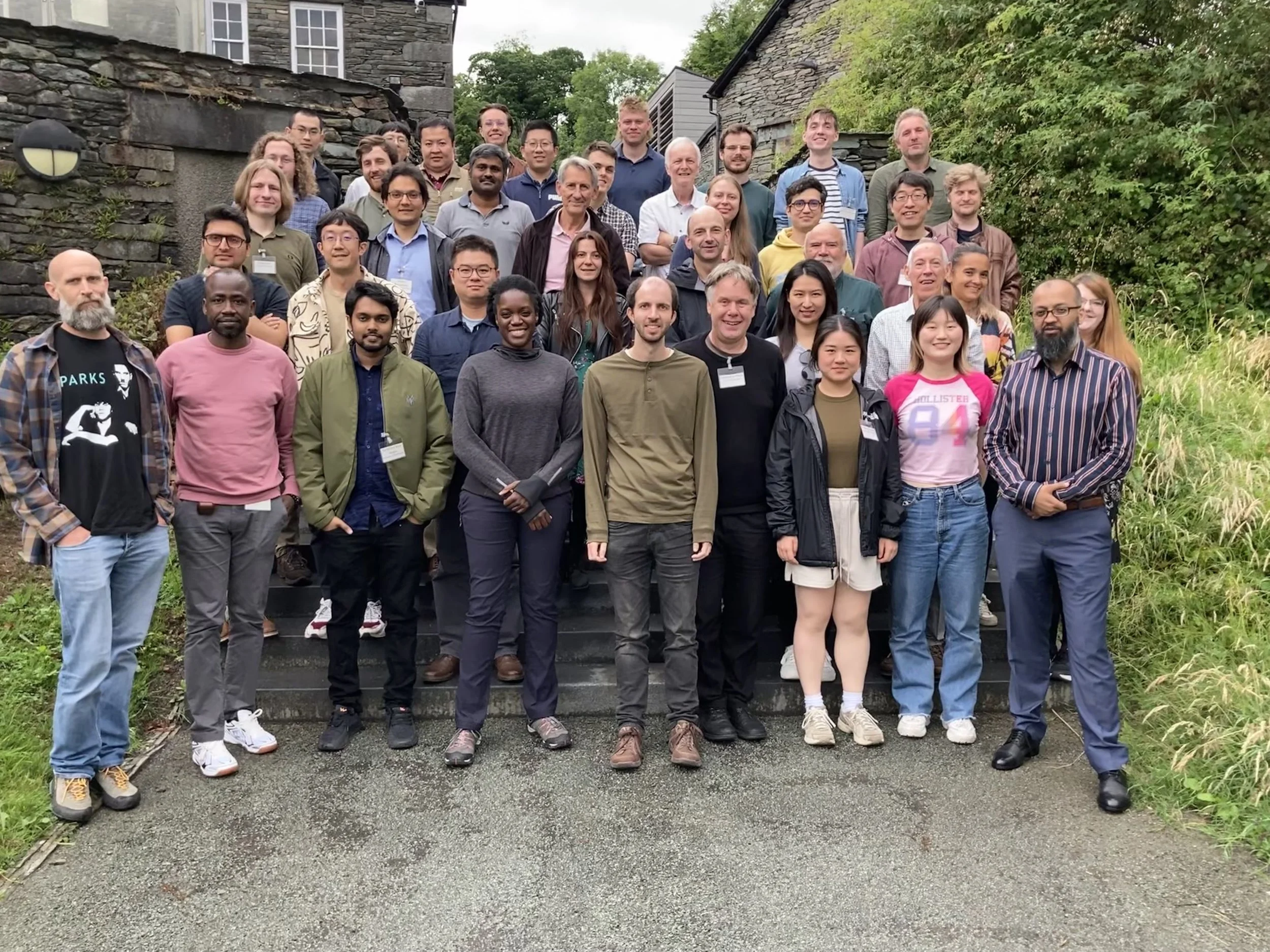
Collaborative excellence: Showcasing the power of our three-university partnership

-
Journal Badge: Communications Materials
Impact Badge: "Top 25 Most Downloaded 2024"
Authors: Acharya R, Coke M, Adshead M, Li K, Achinuq B, Cai R, Gholizadeh A, Jacobs J, Boland J, Haigh S, Moore K, Jamieson D, Curry R
Journal: Communications Materials, Issue 1, 2024
Abstract: Solid-state spin qubits within silicon crystals at mK temperatures show great promise in the realisation of a fully scalable quantum computation platform. Qubit coherence times are limited in natural silicon owing to coupling to the ²⁹Si isotope which has a non-zero nuclear spin. This work presents a method for the depletion of ²⁹Si in localised volumes of natural silicon wafers by irradiation using a 45 keV 28Si focused ion beam with fluences above 1×10^19 ions cm−2. Nanoscale secondary ion mass spectrometry analysis of the irradiated volumes shows residual ²⁹Si concentration down to 2.3 ± 0.7 ppm and with residual C and O comparable to the background concentration in the unimplanted wafer. After annealing, transmission electron microscopy lattice images confirm the solid phase epitaxial re-crystallization of the as-implanted amorphous enriched volume extending over 200 nm in depth.
Impact: This paper was in the top 25 most downloaded research papers of 2024.
-
Journal Badge: Advanced Engineering Materials
Impact Badge: "Editors' Choice - Top 10% Most Viewed"
Authors: Mason Adshead, Maddison Coke, Gianfranco Aresta, Allen Bellew, Matija Lagator, Kexue Li, Yi Cui, Rongsheng Cai, Abdulwahab Almutawa, Sarah J. Haigh, Katie Moore, Nicholas Lockyer, Christopher M. Gourlay, Richard J. Curry
Journal: Advanced Engineering Materials, Volume 25, Issue 22, 2300889 (2023)
Abstract: The ability to spatially control and modify material properties on the nanoscale, including within nanoscale objects themselves, is a fundamental requirement for the development of advanced nanotechnologies. The development of a platform for nanoscale advanced materials engineering (P-NAME) designed to meet this demand is demonstrated. P-NAME delivers a high-resolution focused ion beam system with a coincident scanning electron microscope and secondary electron detection of single-ion implantation events. The isotopic mass-resolution capability of the P-NAME system for a wide range of ion species is demonstrated, offering access to the implantation of isotopes that are vital for nanomaterials engineering and nanofunctionalization. The performance of the isotopic mass selection is independently validated using secondary ion mass spectrometry (SIMS) for a number of species implanted into intrinsic silicon. The SIMS results are shown to be in good agreement with dynamic ion implantation simulations, demonstrating the validity of this simulation approach. The wider performance capabilities of P-NAME, including sub-10 nm ion beam imaging resolution and the ability to perform direct-write ion beam doping and nanoscale ion lithography, are also demonstrated.
Impact: This paper was selected as an Editors' Choice article, handpicked by the editorial team of Advanced Engineering Materials to showcase the very best that the journal has to offer. It was in the top 10% of most-viewed papers published by the journal in 2023.
-
Journal Badge: Applied Physics Letters
Impact Badge: "Featured as Scilight Open Access"
Authors: Wern Ng, Yongqiang Wen, Max Attwood, Daniel C Jones, Mark Oxborro, Neil McN. Alford, Daan M. Arroo
Journal: Appl. Phys. Lett. 124, 044004 (2024)
Abstract: Masers, the microwave analogs of lasers, have seen a renaissance owing to the discovery of gain media that mase at room temperature and zero-applied magnetic field. However, despite the ease with which the devices can be demonstrated under ambient conditions, achieving the ubiquity and portability, which lasers enjoy, has to date remained challenging. We present a maser device with a miniaturized maser cavity, gain material, and laser pump source that fits within the size of a shoebox. The gain medium used is pentacene-doped para-terphenyl, and it is shown to give a strong masing signal with a peak power of −5 dBm even within a smaller form factor. The device is also shown to mase at different frequencies within a small range of 1.5 MHz away from the resonant frequency. The portability and simplicity of the device, which weighs under 5 kg, paves the way for demonstrators particularly in the areas of low-noise amplifiers, quantum sensors, cavity quantum electrodynamics, and long-range communications.
-
Journal Badge: Journal of Applied Physics
Authors: Yongqiang Wen, Philip L. Diggle, Neil McN. Alford, Daan M. Arroo
Journal: J. Appl. Phys. 134, 194501 (2023)
Abstract: The conditions for continuous wave masing are discussed -- the gain medium, the dielectric permittivity and dielectric loss of the resonator, the Purcell factor and the cooperativity. It is shown how the interplay of all these must be balanced carefully in order to breach the threshold for masing and a maser "Phase Diagram" is constructed that combines these parameters.
-
Journal Badge: Scientific Reports
Authors: Timothy Moorsom, Mairi McCauley, Ahmad Nizamuddin Bin Muhammad Mustafa, Sami Ramadan, Joel Burton, Satoshi Sasaki, Donald A. MacLaren & Peter K. Petrov
Journal: Sci Rep 14, 30927 (2024)
Abstract: Topological Insulators (TIs) are promising platforms for Quantum Technology due to their topologically protected surface states (TSS). Plasmonic excitations in TIs are especially interesting both as a method of characterisation for TI heterostructures, and as potential routes to couple optical and spin signals in low-loss devices. Since the electrical properties of the TI surface are critical, tuning TI surfaces is a vital step in developing TI structures that can be applied in real world plasmonic devices. Here, we present a study of Bi₂Se₃/graphene heterostructures, prepared using a low-cost transfer method that reliably produces mono-layer graphene coatings on Bi₂Se₃ flakes. Using both Raman spectroscopy and electron energy loss spectroscopy (EELS), we show that the graphene layer redshifts the energy of the π plasmon mode in Bi₂Se₃, creating a distinct surface plasmon that differs significantly from the behaviour of a TI-trivial insulator boundary. We demonstrate that this is likely due to band-bending and electron transfer between the TI surface and the graphene layer. Based on these results, we outline how graphene overlayers can be used to create tuneable, stable plasmonic materials based on topological insulators.
-
Journal Badge: ACS Applied Materials & Interfaces
Authors: Brock Doiron, Yi Li, Ryan Bower, Andrei Mihai, Stefano Dal Forno, Sarah Fearn, Ludwig Hüttenhofer, Emiliano Cortés, Lesley F. Cohen, Neil M. Alford, Johannes Lischner, Peter Petrov, Stefan A. Maier, Rupert F. Oulton
Journal: ACS Applied Materials & Interfaces 2023 15 (25), 30417-30426
DOI: 10.1021/acsami.3c02812
Abstract: Understanding metal–semiconductor interfaces is critical to the advancement of photocatalysis and sub-bandgap solar energy harvesting where electrons in the metal can be excited by sub-bandgap photons and extracted into the semiconductor. In this work, we compare the electron extraction efficiency across Au/TiO₂ and titanium oxynitride (TiON)/TiO₂–x interfaces, where in the latter case the spontaneously forming oxide layer (TiO₂–x) creates a metal–semiconductor contact. Time-resolved pump–probe spectroscopy is used to study the electron recombination rates in both cases. Unlike the nanosecond recombination lifetimes in Au/TiO₂, we find a bottleneck in the electron relaxation in the TiON system, which we explain using a trap-mediated recombination model. Using this model, we investigate the tunability of the relaxation dynamics with oxygen content in the parent film. The optimized film (TiO₀.₅N₀.₅) exhibits the highest carrier extraction efficiency (NFC ≈ 2.8 × 10¹⁹ m⁻³), slowest trapping, and an appreciable hot electron population reaching the surface oxide (NHE ≈ 1.6 × 10¹⁸ m⁻³). Our results demonstrate the productive role oxygen can play in enhancing electron harvesting and prolonging electron lifetimes, providing an optimized metal–semiconductor interface using only the native oxide of titanium oxynitride.
Our Most Impactful Publications

