Top Trumps
NAME’s Engineering Atom-by-Atom Card Game
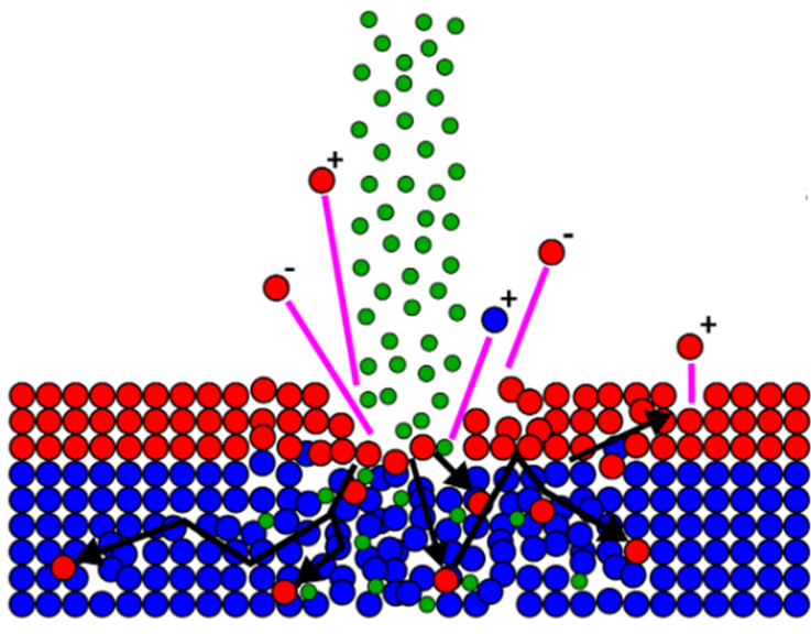
Ion Implantation Applications
We’ve put together 28 different applications of ion implantation, showing just how useful materials modification is, and where you can find it. If you don’t have a pack yet click here to download and print at home.
School Resources
There are many ways to use the card contact us here for our school use sheet to be sent out to you. For tips on using top trumps in the classroom see here.

The Rules
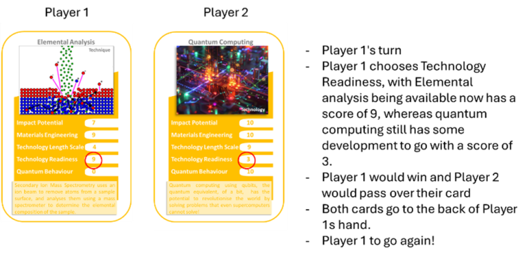
Shuffle the deck and pass out the cards until the whole deck has been dealt out
One person begins by reading out a category such as Readiness or and each player’s cards have a number rating of 1-10 on each category
Then the person with the highest number rating in the chosen category wins the other players card and the winner of that round chooses the next category
This continues until one of the players loses all of their cards
-
![]()
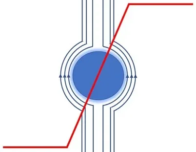
Quantum Time
Ever tried to sync your watch to a friend on the other side of the world? Sure, we use the internet, but all time has to trace back to a ‘master’ clock in a lab somewhere in the world. That clock has to be extremely accurate, and not change its step with time, or else in a few hundred years the time may have jumped one hour! Quantum ‘ion’ clocks made of aluminium ions have offered this unprecedented accuracy, and able to preserve their time for a billion years. To help bring this accuracy to the masses, secondary clocks can be made from hydrogen or solid-state masers, microwave versions of lasers, which have decent time accuracy and more portability. Ion clocks can be explored through the study of metal ion properties, and the time-accuracy of masers could be enhanced through implantation of dopant ions.
-
![]()
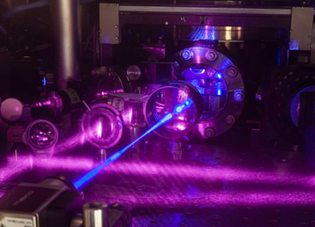
Photonics
Born from Albert Einstein’s Nobel Prize winning discovery of photons, units of light, the field of photonics has enabled scientists to create ‘photonic’ devices essential to the modern world such as lasers and LEDs. Photonics underpins the internet through the fast and long-range fibre-optic transmission of data and is a leading candidate to make quantum computation possible. We have studied light for millennia in a field known as optics, creating devices such as prisms, mirrors and lenses to manipulate it. The field of photonics came about due to Albert Einstein’s discovery that light was made up of units called photons, which a few decades later enabled scientists to create ‘photonic’ devices essential to the modern world such as lasers and LEDs. Photonics underpins the internet through the fast and long-range fibre-optic transmission of data and is a leading candidate to make quantum computation possible.
-
![]()
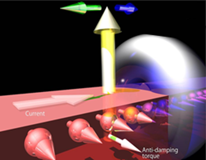
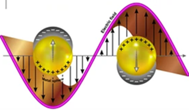
Spin Current
In conventional wires, we transport current with electrons, going from negative to positive. But we can use other properties of electrons to do this transfer more efficiently. Use the power of spin and charge to transport and storage information without heat generation. Spintronics make a difference in comparison to other systems due to electron spins are used as a further degree of freedom, with implications in the efficiency of data storage and transference.
-
![]()
Quantum Computing
Quantum computers are a new type of computing that have the potential to revolutionize the world, as they can solve problems that even today’s best supercomputers would take millions of years to solve. These could range from developing a vaccine in a day to synthesizing a new molecule that could remove carbon from the environment. Like the bit which is the informational building block of classical computers, the qubit is to quantum computers. However, to solve the problems mentioned above these computers need a million qubit so scaling up to these numbers is a serious challenge. This is where Silicon based quantum systems using electron/nuclear spins show great potential as they use the techniques used to make conventional transistor-based electronics like laptops that already show scaling to the billion transistor level!
-
![]()
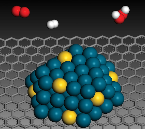
Catalysis
Catalysts are materials that help reduce the energy needed for a chemical reaction, making them more efficient, and sometimes allowing reactions occur that otherwise would not. They are no used up in the reaction, but provide a point where reactants can bond and create intermediates that then undergo the reaction. By using ion implantation we can put these materials directly where we need them, reducing the amount needed, making them more sustainable.
-
![]()
Quantum Sensing
How could we detect the faintest signals from life on other planets? How could we image the inside of the human body quickly for a life-saving diagnostic? Sensors which can access the quantum properties of stimulated emission can amplify these weak signals to powerful levels. The maser, microwave versions of lasers, is such a device that amplifies microwaves and is used in space communication for satellites. Previously only usable at ultra-cold temperatures, a precious few materials have been discovered to mase at room temperature. Ion implantation and material search through using new dopants, could help find new maser materials with stronger amplification, longer amplification times or more robust material properties.
-
![]()
Superconductivity
A Superconductor is a state of matter with zero resistance and unique magnetic properties, like being able to expel all magnetic fields. However, these superconductors require cooling to very low temperatures (-260°C). They have their uses in making ultra-strong magnetics like those in MRI machines or for some designs of quantum computers. A Macroscopic quantum state with zero resistance and unique magnetic properties. They can be used in quantum computers and magnetic levitation trains but require very cold temperatures.
-
![]()
Plasmonics
Plasmonic structures are extremely useful for technology, as they allow light to couple to charge (e.g. electrons in a metal) and be confined to spaces smaller than the wavelength of light. For example, light in the midinfrared range has wavelengths on the order of 10s of microns, yet using plasmonic structures we can confine it to volumes on the order of nanometres (1000 times smaller!). This can lead to strong field enhancements within the plasmonic structure, allowing us to use these structures for nanoscale imaging and sensing. One particular application of plasmonic structures is biosensing, where gold nanoparticles are often used to enhance imaging of biomolecules!
-
![]()
Modelling
Materials modelling allows us to design new materials that provide optimised performance and behaviour. By modelling them we can reduce the number of experiments we need to do and reduce the use of precious chemicals. We can model the materials structure but also the properties so we can optimise the property we are interested in. This can be used for many different types of materials such as materials for solar energy conversion.
-
![]()
Single Photon Emission
Photons are the smallest possible packets of electromagnetic energy. Single photon emitters are things that can only emit one photon at a time, acting as a ‘quantum’ light source. To exhibit this behaviour, the thing emitting light must be very small – trapped single atoms, quantum dots and defects in the structures of solids such as diamond have been used as single photon sources. A photon can act as a ‘qubit’, the basic unit of quantum information, so single photon sources are extremely useful for quantum technologies as they can be used by researchers to generate on-demand qubits, essential for the proposed photonic quantum computers.
-
![]()
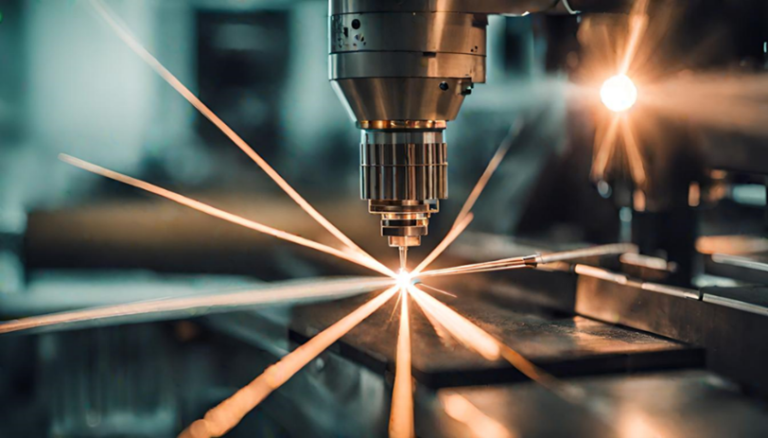
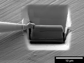
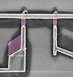
Sample Fabrication
A focused ion beam can be used to make samples very thin. We can take a piece of material we are interested in and remove the material on either side of a slice. Bringing in a needle, we can then pick up this slice of our material and place it into a microscope that uses electron transmission, electrons passing through the thin slice, to observe the structure of the material. As it is so thin we can observe single atoms in the sample using this transmission electron characterisation.
-
![]()
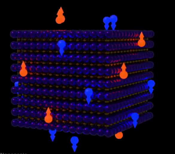
Pure Materials – Enrichment
Isolating qubits (quantum bytes) from environmental sources of noise is one of the most important criteria for the creation of high-quality qubits that can be operated for exceptionally long periods of time. The surrounding natural occurring spins in the qubit material of choice i.e. Silicon can “talk” to the qubit and lead the qubit to no longer be useful. Isotopic purification of the environment which removes these crowd of spins around the central qubit leads to exceptionally long coherent high-quality qubits by creating a spin-free environment.
-
![]()
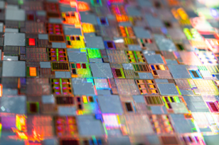
Semiconductors
Semiconductors underpin modern electronic technologies. Many of our semiconductor technology is based on silicon chips that are a combination of transistors and other components. The development of silicon transistors has followed a trend known as Moore’s Law, doubling the number of transistors every 2 years. Rather than a law of physics, it is an empirical relationship that has held true for transistors on a chip. Various different technologies are used in the manufacture of these chips, including focused ion beams.
-
![]()
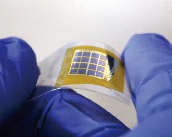
Solar Cells
Solar cells have the ability to use light and convert to electricity. A clear top layer allows sunlight to fall on an energy conversion layer. The material chosen to convert the energy, absorbs the light and produces streams of negatively charged electrons and positively charged holes moving in opposite directions. Having direct control over layers enables the production of different areas that interact with the light differently so we can affect how effective our cell is.
-
![]()
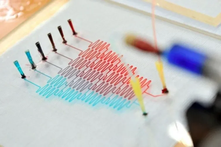
Microfluidics
Microfluidics
is the science that studies the behaviour of fluids through micro-channels. By
having micro-channels, we can change the way the fluid flows and introduce
chemicals at very precise rates. By using ion implantation, we can
functionalize the channels, creating different chemical reactions under different
conditions. We can also integrating electronic devices with these channels
enabling technologies such as biological sensing to be developed.By only having
the functional material in the precise area as needed, we can also move to
using less material, making the use of them greener which is important for rare
materials.
Picture credit; Nichole Pamme -
![]()
Elemental Analysis
Secondary Ion Mass Spectrometry (SIMS) uses an ion beam to bombard the sample surface and remove material from a sample. A portion of the material removed from the surface is ionised and these secondary ions are sent into a mass spectrometer so that their mass can be determined. By scanning the beam over the sample it is possible to build up a chemical map of the elements and isotopes on the surface of the sample. Repeatedly scanning the ion beam over the same part of the sample allows a depth profile to be generated to give an indication of the chemistry of the sample in depth. Typical application areas include semiconductors, materials science, biology and geology.
-
![]()
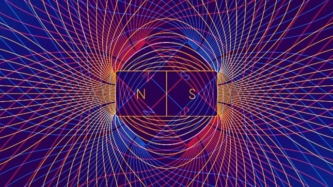
Magnetic Material
Magnetism is caused by the arrangement electron spins, and also electron motion (current). Magnetic materials have many uses from fridge magnets through to computer memory. In a classical magnet, there is a north and south pole, where opposites attract and similar repel. Using different alloys, and mixing different metals, we can adjust the strength and location of the magnetic field created by these permanent magnetic materials.
-
![]()
Standards
A standard is a defined relationship to a unit of measurement of e.g., time, mass or length. Standards are the fundamental reference for which against all other measuring devices are compared. Historical standards for length, volume, and mass were defined by many different authorities, which resulted in confusion and inaccuracy of measurements. As we need to measure things more precisely, we need to improve the precision of our reference standards and make sure they are the same all over the world.
-
![]()
Anti-microbial Surfaces
Anti-microbial surfaces have a coating that stops the growth of microorganisms on a material.
This can help reduce the spread of viruses that are touched frequently by many people. By optimizing the properties, we can make the surfaces more efficient at either repelling or killing potentially harmful microorganisms. -
![]()
Corrosion Resistance
Preventing surfaces from corroding is key to prolonging a material’s lifespan and reduces waste, making them sustainable. We can prevent corrosion by adding new atoms to change the surface chemistry. By adding only to the surface we can keep the bulk properties of the material we are interested in. Depending on the environment, what chemicals are present, temperature or acidity, the type of anti-corrosion will vary and may be barrier resistance, where the layer creates a barrier through not being chemically active in that environment or sacrificial where the top layer is sacrificed but in doing so create a barrier to the bulk.
-
![]()
Chemical Sensing
Detecting the presence of chemicals is vital to understanding our environment. Even the smallest amounts of some chemicals can be dangerous, but also the smallest of changes in chemicals can give us an insight into larger changes in the environment. New quantum sensors will improve our ability to monitor our world.
-
![]()
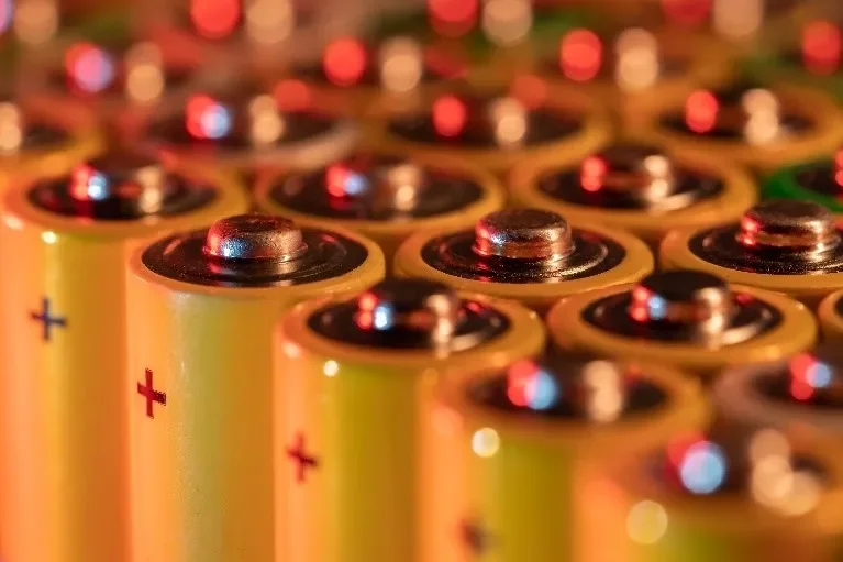
Energy Storage
Energy needs to be stored in a way that allows it to be used later. This is important for transient energy sources such as solar energy, where we have an abundance at one time, during the day, and less at another, at night. But also important for safe portable devices that are commonplace. Making materials that can store and dissipate energy efficiently is key so that as much of this energy is converted into a usable form.
-
![]()
Energy Conversion
Energy can be stored in many forms, from heat to chemical potential. We need materials to convert between them so they can be used efficiently and accessed on demand. This may require many steps so it is important that each material involved is optimised so reduce the loss in the system.
-
![]()
Functional 2D Materials
2D materials are made from single sheets of connected atoms. Controlling the composition of the 2D sheet strongly changes the physical properties. Graphene was the first 2D material to be isolated at the University of Manchester. Using tape and graphite, you are able to overcome the weak intramolecular forces connecting the sheets of carbon and peel off single layers of carbon in the form of graphene. Compared to the bulk, where we have a large amount of the material, 2D materials have different properties. Graphene stands out for being tough, flexible, light, and with a high resistance. It’s calculated that this material is 200 times more resistant than steel and five times lighter than aluminum. With these properties, graphene has applications in the energy, construction, health, and electronics sectors
-
![]()
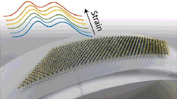
Strain Engineering
Stress refers to the force applied to a material per unit area. Strain in a material is the equivalent of applying pressure and allows us to control the colour of semiconductor lasers. The barcode scanner in a supermarket was one of the first strained-layer laser products.
-
![]()
Imaging
Imaging can be done across length scales ranging from nanometers to kilometres using different techniques. When you bombard a surface of a material with electrons or ions (charged atoms), the surface will eject electrons which you can detect and construct an image of the surface from. If you bombard a very thin material and observe how electrons travel through the material, transmit, it allows us to image the smallest objects, even single atoms!
-
![]()
Device Fabrication
The use of electrons, photons and even ions (charged atoms) to pattern materials is called lithography. Once patterned, the material changes its chemical selectivity to either harden or become susceptible to being washed away, leaving the pattern in the material. One of the most common material used for this are polymer resists. This is used to fabricate devices across different length scales from nanometers to micrometers, especially in the semiconductor industry.
-
![]()
Topological Insulators
A topological insulator is a material whose interior behaves as an electrical insulator while its surface behaves as an electrical conductor. Topological insulators may offer a future efficient route to computing. Their protected surface states, that are used to transfer information, cannot be broken, and therefore reduce error! These surface states are surface bound and therefore the middle or bulk of the material acts differently, being an electrical insulator.